
www.industryemea.com
12
'26
Written on Modified on
CeramTec at SEMICON India 2026
From from 17 to 19 September, in Yashobhoomi, Delhi, CeramTec collaborates with equipment manufacturers to implement advanced technical ceramics for process stability and thermal management.
www.ceramtec-group.com
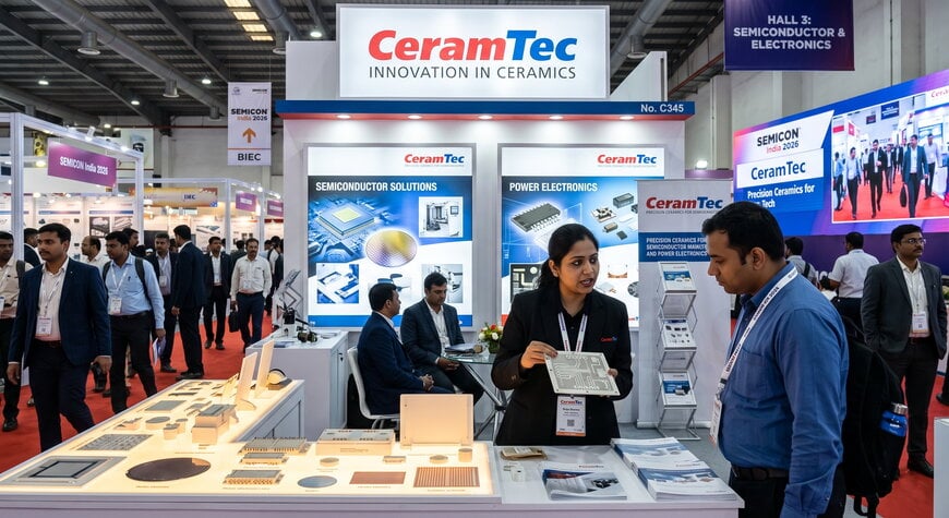
A technical cooperation between CeramTec and equipment manufacturers addresses high-stress requirements in semiconductor manufacturing and power electronics infrastructure. The partnership focuses on deploying high-precision ceramic components and substrates to meet mechanical tolerance, chemical resistance, and thermal dissipation requirements across industrial applications.
Industrial Challenge in Semiconductor Manufacturing
Modern wafer processing involves harsh process conditions, including plasma exposure, aggressive chemical etching, elevated thermal cycles, and strict particle contamination thresholds. Standard metal or polymer components frequently experience rapid degradation, leading to process drift, particle release, and unplanned downtime. To stabilize wafer handling, etching, deposition, and metrology systems, manufacturers require structural materials with high mechanical hardness, low thermal expansion, and resistance to chemical attack.
Cooperation Strategy and Technical Roles
Equipment integration demands precise material selection paired with custom machining capabilities. While equipment manufacturers define functional architectures and operational tolerances, CeramTec provides material engineering, precision grinding, lapping, and polishing to achieve strict dimensional tolerances and defined surface roughness parameters.
Technical Substrate Solutions and Properties
The technical framework utilizes four distinct substrate materials designed for electrical insulation and thermal dissipation in high-power applications:
- Aluminum Oxide: Provides balanced mechanical strength and dielectric properties for standard electronic circuit isolation.
- Aluminum Nitride: Offers high thermal conductivity exceeding 170 W/mK for intense heat dissipation requirements.
- Zirconia Toughened Alumina: Enhances mechanical toughness and flexural strength to prevent mechanical fracture under structural loads.
- Silicon Nitride: Combines high mechanical strength, resistance to thermal shock, and high fatigue resistance for extreme electrical and thermal stress cycles.
Implementation and Application Scope
The components are integrated directly into structural and electrical subsystems used in power generation, industrial drive systems, energy storage, charging infrastructure, and electronic mobility. In process tools, ceramic parts serve as structural guides, wafer holders, and chamber components where dimensional stability prevents mechanical misalignment during thermal processing.
The performance of these materials was presented at SEMICON India from 17 to 19 September 2026 at Yashobhoomi in Delhi, India, highlighting implementation strategies for regional manufacturing infrastructure.
Measurable Process Impacts
Using specialized technical ceramics provides measurable operational improvements:
The components are integrated directly into structural and electrical subsystems used in power generation, industrial drive systems, energy storage, charging infrastructure, and electronic mobility. In process tools, ceramic parts serve as structural guides, wafer holders, and chamber components where dimensional stability prevents mechanical misalignment during thermal processing.
The performance of these materials was presented at SEMICON India from 17 to 19 September 2026 at Yashobhoomi in Delhi, India, highlighting implementation strategies for regional manufacturing infrastructure.
Measurable Process Impacts
Using specialized technical ceramics provides measurable operational improvements:
- Extended Component Lifespan: High plasma and chemical resistance reduces component degradation and replacement intervals in etching and deposition chambers.
- Thermal Efficiency: High-conductivity substrates reduce thermal resistance, maintaining junction temperatures within specified thresholds in power module architectures.
- Dimensional Accuracy: Surface finishing via lapping and polishing yields tight physical tolerances, preventing particle entrapment and maintaining uniform contact during wafer processing.
