
www.industryemea.com
17
'26
Written on Modified on
300 mm PVD System For Quantum Semiconductor Manufacturing
Fraunhofer IPMS integrates Polyteknik's Flextura PVD system to develop and qualify superconducting materials for quantum processors within industrial semiconductor manufacturing environments.
www.fraunhofer.de
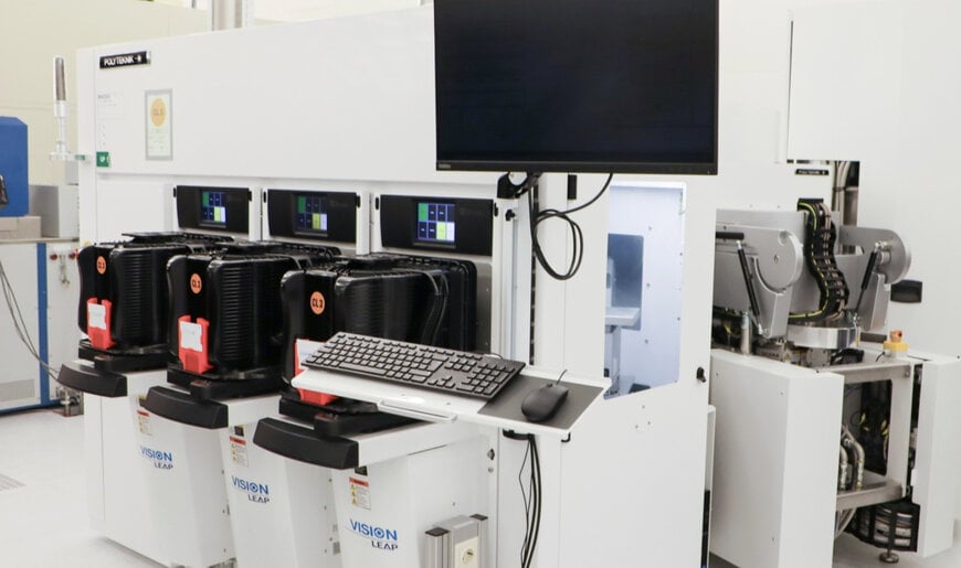
Fraunhofer IPMS has implemented a new physical vapor deposition system to bridge fundamental materials research and industrial semiconductor manufacturing. The deployment targets the development of complex material stacks required for future quantum computing architectures.
Addressing the Industrial Challenge
Scalable quantum computing demands manufacturing technologies capable of combining high material quality with production processes compatible with standard semiconductor fabrication. Transitioning from laboratory-scale research to high-volume industrial manufacturing requires specialized infrastructure. To address this, Fraunhofer IPMS expanded its capabilities to secure a qualified research and development environment that allows industrial partners to evaluate innovative device concepts under conditions closely resembling future mass production.
Technical Architecture and Responsibilities
Polyteknik supplied the Flextura PVD system, which integrates multiple deposition technologies for developing complex material stacks consisting of metals, nitrides, and oxides. The platform is designed to deposit superconducting materials, specifically niobium nitride and zirconium nitride, directly onto standard 300 mm wafers. The system is engineered to achieve benchmark properties with higher deposition rates and stringent film uniformity. Prof. Dr. Wenke Weinreich, Institute Director of Fraunhofer IPMS, stated that scalable quantum computing requires manufacturing technologies that combine outstanding material quality with semiconductor-compatible production processes, and that the new PVD platform expands the institute's capabilities to develop and qualify superconducting materials under CMOS-compatible conditions.
Deployment and Operational Integration
The physical vapor deposition platform is fully integrated into the 300 mm cleanroom environment at Fraunhofer IPMS. The installation complements the existing process portfolio of the institute within the Research Fab Microelectronics Germany. Furthermore, the infrastructure supports major European pilot line initiatives, including APECS, SUPREME, and SPINS, which aim to reinforce the regional semiconductor and quantum technology ecosystem.
Applications and Use Cases
The material combinations developed on this platform form the foundation for superconducting circuits and critical devices required for next-generation quantum processors. Beyond internal research, the expanded infrastructure provides industrial partners with direct access to a qualified 300 mm R&D environment for process validation, material qualification, and continuous technology refinement.
Results and Expected Impact
Initial process developments have demonstrated superconducting properties for niobium nitride and zirconium nitride deposited directly on 300 mm wafers. The engineering results show material characteristics consistent with values reported in scientific literature, validating the platform's capability to transfer high-performance quantum materials into an industrial wafer format. This technological integration establishes a major operational milestone in setting up a European Quantum Research Foundry for advanced semiconductor infrastructure.
Edited by Maria Brueva, Induportals editor – adapted by AI.
www.ipms.fraunhofer.com
