www.industryemea.com
02
'25
Written on Modified on
IDS: See. Align. Place
Precision vision systems power Micro-LED bonding and HBM packaging.
en.ids-imaging.com
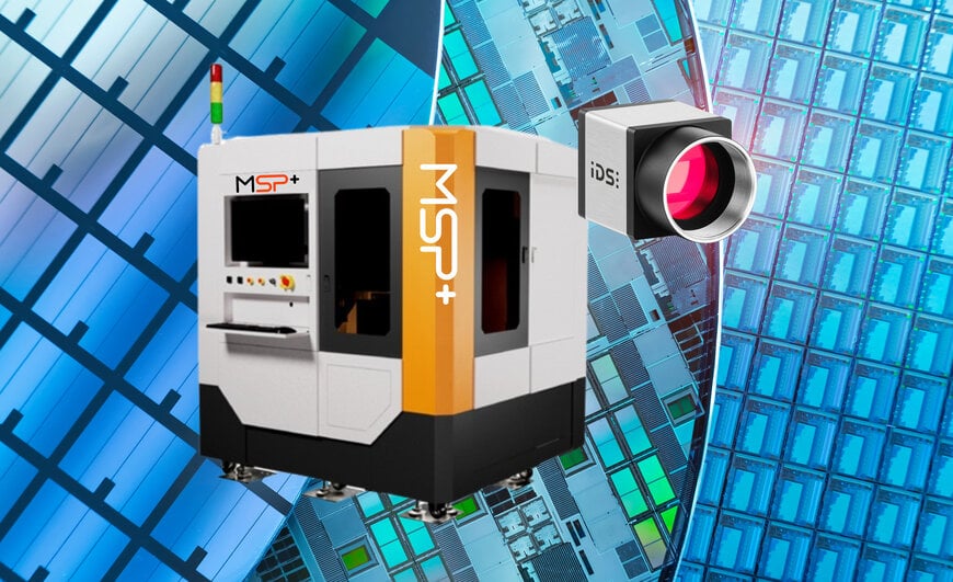
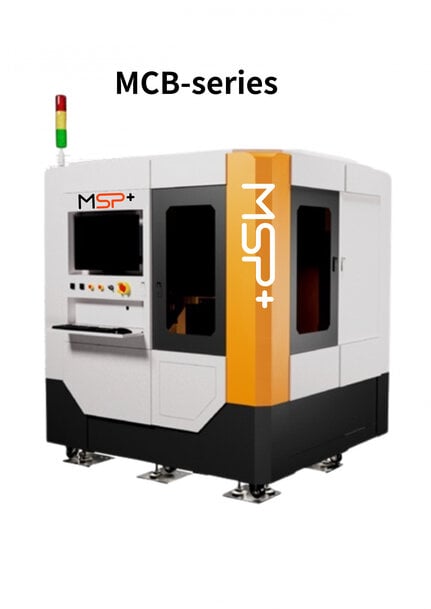
As Micro-LED displays and advanced semiconductor components push the limits of miniaturization and efficiency, precision and scalability in manufacturing become critical. The technology‑leading company Micraft Systems Plus has developed two cutting-edge systems that meet these demands: the uLED Laser Soldering Machine and the HBM High-Accuracy Die Bonder. Both rely on industrial cameras from the USB3 uEye CP series from IDS Imaging Development Systems to deliver maximum accuracy, speed, and process control. These systems are already in high-volume use across the Asian electronics market.
Application 1: Micro-LED Transfer & Laser Soldering with 20MP USB3 uEye CP cameras
The uLED Laser Soldering Machine is designed for high-speed, precise of Micro-LEDs onto large-area substrates including G4.5 and G6 glass panels. Laser soldering minimizes thermal and mechanical stress, which is essential when handling thousands of miniature components simultaneously.
Firstly, the cameras are used to capture global reference marks for the preliminary alignment or to determine the rough position of the substrate in the machine coordinate system. This position data is then transmitted to the motion control system, which enables high-precision motion control on this basis - with a repeat accuracy of the coordinates of around ±1 µm.
Once qualified, the chips are aligned and transferred with extreme precision. For fine adjustment, the cameras now capture fiducial marks, enabling real-time sub-micrometer alignment of the substrate and, if necessary, dynamic rotation correction. The alignment results are then transmitted to the motion control system, which adjusts the stage position and angle to ensure each Micro-LED is perfectly matched to the target location.
With a throughput rate of up to 10 million chips per hour, the system delivers both exceptional accuracy and high-volume efficiency, a key performance indicator (KPI) for scalable mass production.
After bonding, the camera automatically moves to the relevant area, enabling operators to perform an initial inline visual inspection - such as verifying chip alignment, detecting potential tilt, and checking for physical damage or placement errors. This step is critical in mass transfer operations where yield optimization is essential.
USB3 uEye CP industrial cameras from IDS are the sharp eyes of the uLED Laser Soldering Machine from MSP
Advanced camera tasks in the micro LED process:
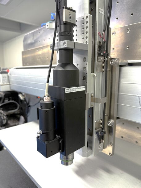
USB3 uEye CP cameras from IDS are the eyes of the uLED Laser Soldering Machine. Throughout the Micro LED workflow, the two integrated U3-3800CP-M-GL Rev.2.2 cameras from IDS support several key process steps:
- Donor wafer inspection (prior to transfer): Cameras detect defects such as cracks or missing units, ensuring only functional Micro LED chips are selected.
- Alignment and placement (during mass transfer): Cameras identify alignment marks and fiducials on substrates and dies. The results are transmitted to the motion control system for sub-micron placement accuracy.
- Post-transfer inspection: The cameras verify that each Micro LED has been precisely positioned and is free of tilt, damage, or misplacement.
- Rework and repair: When necessary, cameras guide pick-and-place systems to replace individual chips with precision.
“Exceptionally high-resolution images with low noise levels ensure the capture of even the smallest details”, emphasises Damien Wang, Area Sales Manager APAC South East at IDS. The light-sensitive IMX183 Rolling Shutter CMOS Sensor from Sony's STARVIS series in the USB3 Vision industrial camera U3-3800CP Rev.2.2.provides outstanding image quality with a resolution of 20.44 MP (5536 x 3692) at 2.4 µm pixels and it delivers up to 19.8 fps.
The camera is therefore ideally suited for complex image analysis in applications such as surface and display inspections.
Application 2: Die Bonding for High Bandwidth Memory (HBM) with 12MP USB3 uEye CP cameras
The second system, the HBM High-Accuracy Die Bonder, is designed for advanced semiconductor packaging, especially HBM (High Bandwidth Memory) applications where vertical stacking of dies requires micron-level precision.
Here, two U3-3890CP-M-GL Rev.2.2 cameras from IDS locate the dies and bonding pads, provide precise coordinates to the placement unit, and enable accurate placement of each component. “The IDS camera is also mainly used for the alignment system in our HBM equipment. It identifies the positions of the chip and the target substrate and converts this information into coordinates for the motion control system to achieve precise positioning and alignment”, explains the manufacturer. The control unit uses these coordinates to guide placement with sub-micron accuracy, ensuring consistent results in high-density packaging.
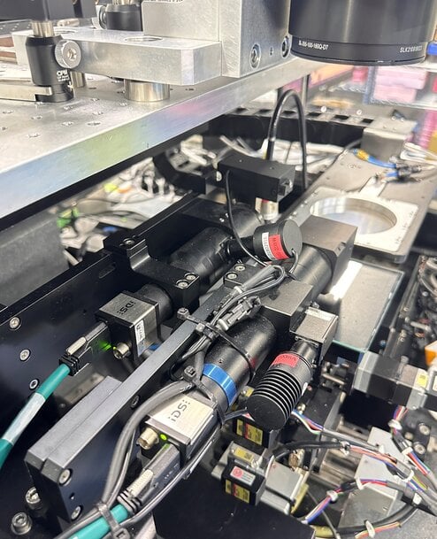
Two U3-3890CP-M-GL Rev.2.2 cameras from IDS identify the uLED chip location
Inline inspection checks every bond for placement accuracy, alignment integrity, and possible damage. In high-density memory stacks, even minor misalignments can lead to electrical or thermal issues, making precise vision a must.
Sensor performance for precise bonding
The U3-3890CP Rev.2.2 is equipped with the rolling shutter CMOS sensor IMX226. The 12.00 MP sensor (4000 x 3000 px, pixel size 1.85 µm) from the Sony STARVIS series excels with exceptional light sensitivity and low noise levels. At full resolution, it delivers a frame rate of 33.2 fps. - perfect for fast, precise processes. Thanks to IDS camera integration, the system achieves repeatable accuracy and long-term process stability - ideal for complex 2.5D or 3D semiconductor packages.
Vision Technology at the Core: IDS uEye CP Cameras
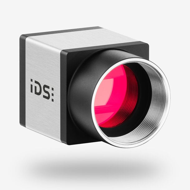
To achieve the required speed and precision, both systems count on IDS’s uEye CP camera series. These compact (29 × 29 × 29 mm) cameras are built for industrial environments, featuring durable magnesium housing, Global Shutter CMOS sensors, and USB3 Vision connectivity. Thanks to the STARVIS series BSI ("back-side-illumination") technology, both sensors are ideally suited for tasks that require a perfect result even in low light conditions. Their high-resolution, low-noise imaging allows reliable detection of alignment marks, micro chip positions, solder bumps, and post-bonding joint quality, even at sub-micron scale. Crucially, their fast frame rate and minimal latency ensure seamless interaction with motion-control systems, providing real-time image data for rapid adjustments. These cameras also demonstrate strong thermal reliability, supporting continuous 24/7 operation essential in semiconductor factories.
The standby mode reduces the power consumption in idle mode to a minimum and thus contributes to energy efficiency, making the industrial camera an environmentally friendly solution for long-term use.
With the comprehensive software SDK from IDS, integration and on-site calibration become simple, making the uEye CP a foundational enabler for precision and throughput in packaging processes.
Customer Benefit: Scalable Precision and Increased Efficiency
By integrating IDS vision technology into both platforms, the machine builder significantly enhanced process accuracy, repeatability, and reliability. Error rates fell, setup times shortened, and overall manufacturing efficiency improved - driving strong competitive advantage in both Micro‑LED displays and advanced semiconductor packaging.
Both systems are already in use with leading manufacturers in Taiwan and Asia, showcasing how German-engineered vision technology seamlessly integrates with state-of-the-art automation to meet modern production demands.
Outlook
The market for semiconductor manufacturing – particularly in precision automation – is developing rapidly, and with it, the requirements for modern industrial cameras are also evolving. “Our customers are demanding high-resolution, compact, and absolutely reliable solutions more than ever before,” says Damien Wang.
The trend toward higher resolution is a key driver of innovation: sharp, detailed images are essential for complex automation tasks. At the same time, stable performance under challenging operating conditions has become a fundamental requirement. “Many applications require continuous, uninterrupted operation. That’s why our focus is increasingly on cameras that perform reliably even in demanding environments,” emphasizes the responsible project manager from Micraft Systems Plus.
Another trend is ongoing miniaturization. Industrial cameras with compact form factors are gaining importance, as space in modern systems is often limited – without any compromise in performance.
To address these developments, the product portfolio is being strategically expanded and adapted to meet the growing technical demands.
The camera is therefore ideally suited for complex image analysis in applications such as surface and display inspections.
Application 2: Die Bonding for High Bandwidth Memory (HBM) with 12MP USB3 uEye CP cameras
The second system, the HBM High-Accuracy Die Bonder, is designed for advanced semiconductor packaging, especially HBM (High Bandwidth Memory) applications where vertical stacking of dies requires micron-level precision.
Here, two U3-3890CP-M-GL Rev.2.2 cameras from IDS locate the dies and bonding pads, provide precise coordinates to the placement unit, and enable accurate placement of each component. “The IDS camera is also mainly used for the alignment system in our HBM equipment. It identifies the positions of the chip and the target substrate and converts this information into coordinates for the motion control system to achieve precise positioning and alignment”, explains the manufacturer. The control unit uses these coordinates to guide placement with sub-micron accuracy, ensuring consistent results in high-density packaging.
Two U3-3890CP-M-GL Rev.2.2 cameras from IDS identify the uLED chip location
Inline inspection checks every bond for placement accuracy, alignment integrity, and possible damage. In high-density memory stacks, even minor misalignments can lead to electrical or thermal issues, making precise vision a must.
Sensor performance for precise bonding
The U3-3890CP Rev.2.2 is equipped with the rolling shutter CMOS sensor IMX226. The 12.00 MP sensor (4000 x 3000 px, pixel size 1.85 µm) from the Sony STARVIS series excels with exceptional light sensitivity and low noise levels. At full resolution, it delivers a frame rate of 33.2 fps. - perfect for fast, precise processes. Thanks to IDS camera integration, the system achieves repeatable accuracy and long-term process stability - ideal for complex 2.5D or 3D semiconductor packages.
Vision Technology at the Core: IDS uEye CP Cameras
To achieve the required speed and precision, both systems count on IDS’s uEye CP camera series. These compact (29 × 29 × 29 mm) cameras are built for industrial environments, featuring durable magnesium housing, Global Shutter CMOS sensors, and USB3 Vision connectivity. Thanks to the STARVIS series BSI ("back-side-illumination") technology, both sensors are ideally suited for tasks that require a perfect result even in low light conditions. Their high-resolution, low-noise imaging allows reliable detection of alignment marks, micro chip positions, solder bumps, and post-bonding joint quality, even at sub-micron scale. Crucially, their fast frame rate and minimal latency ensure seamless interaction with motion-control systems, providing real-time image data for rapid adjustments. These cameras also demonstrate strong thermal reliability, supporting continuous 24/7 operation essential in semiconductor factories.
The standby mode reduces the power consumption in idle mode to a minimum and thus contributes to energy efficiency, making the industrial camera an environmentally friendly solution for long-term use.
With the comprehensive software SDK from IDS, integration and on-site calibration become simple, making the uEye CP a foundational enabler for precision and throughput in packaging processes.
Customer Benefit: Scalable Precision and Increased Efficiency
By integrating IDS vision technology into both platforms, the machine builder significantly enhanced process accuracy, repeatability, and reliability. Error rates fell, setup times shortened, and overall manufacturing efficiency improved - driving strong competitive advantage in both Micro‑LED displays and advanced semiconductor packaging.
Both systems are already in use with leading manufacturers in Taiwan and Asia, showcasing how German-engineered vision technology seamlessly integrates with state-of-the-art automation to meet modern production demands.
Outlook
The market for semiconductor manufacturing – particularly in precision automation – is developing rapidly, and with it, the requirements for modern industrial cameras are also evolving. “Our customers are demanding high-resolution, compact, and absolutely reliable solutions more than ever before,” says Damien Wang.
The trend toward higher resolution is a key driver of innovation: sharp, detailed images are essential for complex automation tasks. At the same time, stable performance under challenging operating conditions has become a fundamental requirement. “Many applications require continuous, uninterrupted operation. That’s why our focus is increasingly on cameras that perform reliably even in demanding environments,” emphasizes the responsible project manager from Micraft Systems Plus.
Another trend is ongoing miniaturization. Industrial cameras with compact form factors are gaining importance, as space in modern systems is often limited – without any compromise in performance.
To address these developments, the product portfolio is being strategically expanded and adapted to meet the growing technical demands.