www.industryemea.com
28
'22
Written on Modified on
Nexperia’s 50 µA Zener diodes portfolio extends battery-time and saves PCB space
The comprehensive product range covers every application from 1.8 V to 75 V.

Nexperia, the expert in essential semiconductors, today announced a comprehensive range of low current voltage regulator diodes. The 50 µA Zener diode range is available in three different surface-mountable (SMD) package options, in an ultra-small Discretes Flat No-leads (DFN) package and AEC-Q101 qualified parts, providing the ultimate in customer choice and flexibility. Specified at a low test current (50 μA), the efficient diodes are ideal for low bias and portable battery-powered devices in mobile, wearable, automotive and industrial applications.
“The DFN1006BD-2 packaged parts with side-wettable flanks (SWF) address the concerns of various sectors, such as size, performance and ruggedness, and match many diverse applications,” says Paula Stümer, product manager at Nexperia. “Covering a wide 1.8 V to 75 V range, we deliver the industry’s broadest 50 μA Zener diode portfolio in DFN technology. However, parts are also available in leaded SMD styles, giving customers the flexibility of choice.”
With 40 new types per package option covering nominal working voltages from 1.8 V to 75 V, the range is available in the ultra-low profile surface-mountable SOT23 (BZX8450), SOD323 (BZX38450) and SOD523 packages (BZX58550) and leadless DFN1006BD-2 (BZX8850S) package. The Zeners feature a non-repetitive peak reverse power dissipation of ≤40 W, total power dissipation ≤300 mW and low dynamic resistance. They are also available as Q-portfolio parts, meeting the AEC-Q101 and ISO/TS16949 automotive quality standards. As more non-automotive applications require additional quality-related services, such as PPAP (Production Part Approval Process) and extended longevity, these Q-portfolio parts fulfil this need.
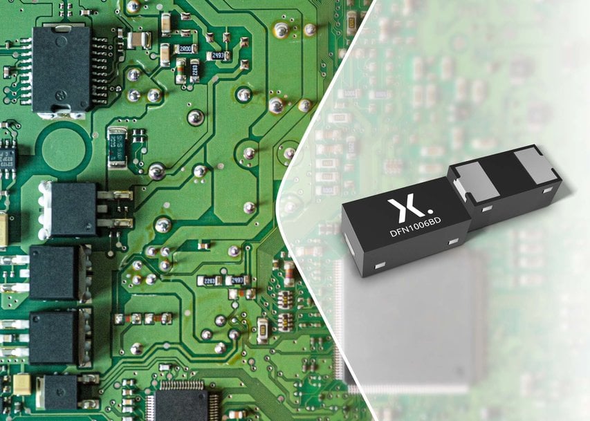
The DFN package with compact dimensions (1.0 mm x 0.6 mm x 0.47 mm) is the right choice for replacing bulky leaded packages on PCBs and can save up to 60% in space. It features side-wettable flanks (SWF), which ensure the solder flows up the side of the chip when it is soldered onto the PCB. This technology facilitates automated optical inspection (AOI), satisfying the automotive industry’s high safety, reliability and quality requirements. The high P(tot) of the DFN-packaged Zeners also run cooler than leaded parts, therefore improving system reliability.
Nexperia continues to invest in developing new technologies and increasing in-house manufacturing capacity. The 50 µA Zeners are already available as samples and in volume production quantities. For more information, including product specifications and datasheets, please visit: www.nexperia.com/50-microA-zener
www.nexperia.com

