
Navitas Powers AI and EVs with Gen-3 ‘Fast’ SiC in Robust TOLL Package
3rd gen 650 V ‘fast’ silicon carbide (SiC) MOSFETs deliver highest power density in robust, thermally enhanced packaging for critical, high-reliability, high-efficiency applications.
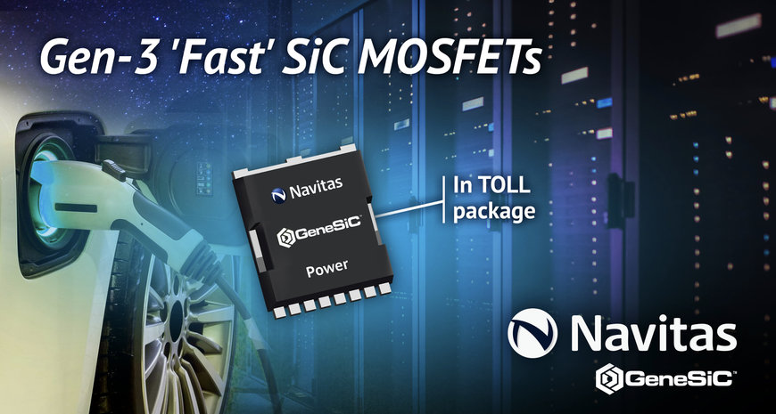
Navitas Semiconductor, the industry leader in next-generation GaNFast™ gallium nitride (GaN) and GeneSiC™ silicon carbide (SiC) power semiconductors, has extended its new portfolio of Gen-3 ‘Fast’ (G3F) 650 V SiC MOSFETs into a thermally-enhanced, rugged, high-speed, surface-mount TOLL (Transistor Outline Leadless) package designed for demanding, high-power, high-reliability applications.
Combining high-power capability and best-in-class low on-resistance of 20 to 55 mΩ, these 650 V SiC MOSFETs have been optimized for the fastest switching speed, highest efficiency, and increased power density demanded by applications such as AI data center power supplies, EV charging and energy storage and solar solutions (ESS).
Navitas’ GeneSiC products use a proprietary ‘trench-assisted planar’ technology that provides world-leading efficiency performance over the temperature range, with G3F MOSFETs delivering high-speed, cool-running performance that ensures up to 25°C lower case temperatures and up to 3x longer life than alternative SiC products.
Navitas’ latest 4.5 kW AI power system reference design features the G3F45MT60L (650V 40 mΩ, TOLL) G3F SiC MOSFET in an interleaved CCM-TP PFC topology. Complemented by the NV6515 (650V, 35mΩ, TOLL) GaNSafe™ Power IC in the LLC stage, the 4.5 kW solution has a peak efficiency above 97% and, at 137 W/inch3, it is the world’s highest power density AI PSU. For 400 V-rated EV battery systems, G3F in TOLL is an ideal technology for on-board chargers (OBC), DC-DC converters, and traction drives ranging from 6.6 to 22 kW.
The surface-mount TOLL package offers a 9% reduction in junction-to-case thermal resistance (RTH,J-C), 30% smaller PCB footprint, 50% lower height, and 60% smaller size than the traditional D2PAK-7L, enabling highest-power-density solutions, as demonstrated in the 4.5 kW AI solution. Additionally, with a minimal package inductance of only 2 nH, excellent fast-switching performance and lowest dynamic losses are achieved.
www.navitassemi.com
